1.Fabrication:
The combination of o-SPL and dry etching processes to define and transfer SiO2 mask lines on the active layer of a silicon on insulator (SOI) is used to obtain SiNW field-effect transistors with widths in the range of 20-100 nm. The heights of the nanowires will be given by the thickness of the silicon layer of the starting SOI.
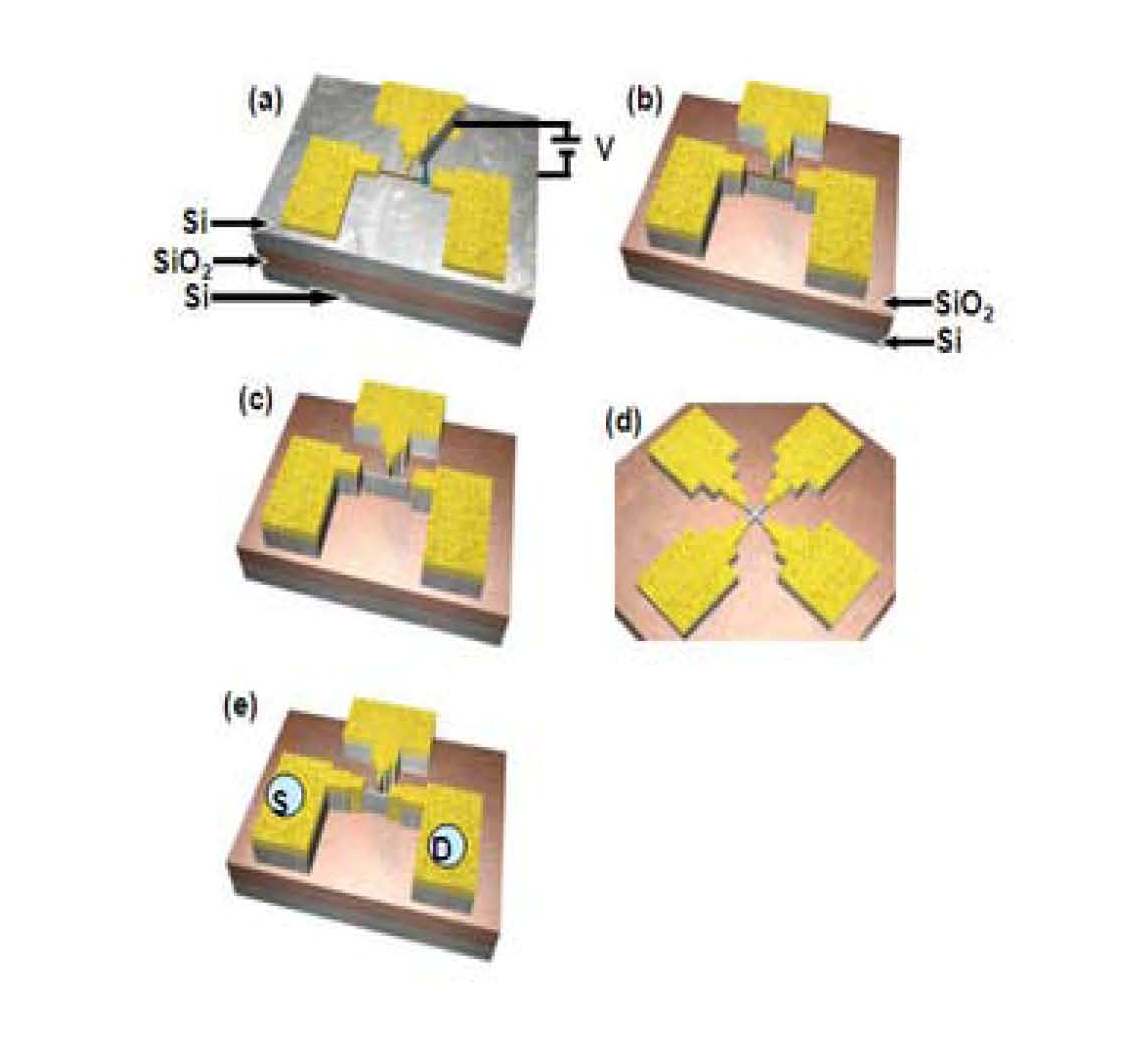
Fig 1. Fabrication Process of the o-SPL SiNW FETs
2.Electrical characterization
The transistor curves and electric characteristics of the devices are measured at room temperature with a probe station.
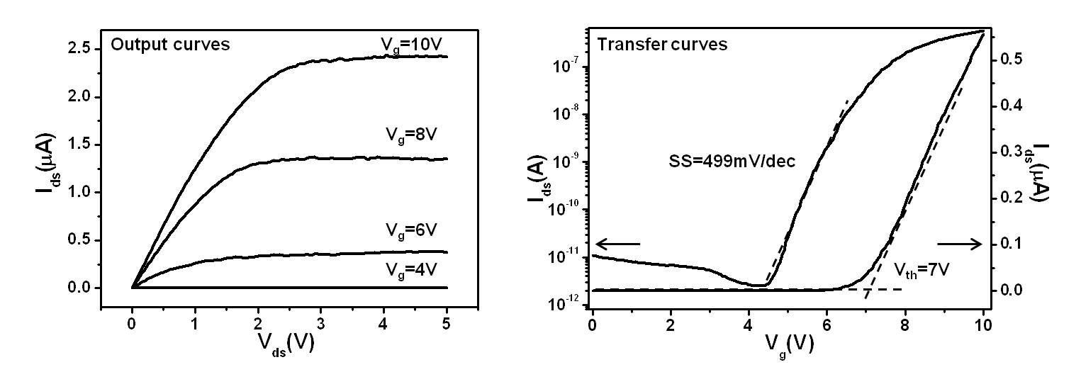
Fig. 2. Transistor curves of a typical device
3.Label-free biosensor
o-SPL SiNW FETs have been used for the detection of molecular recognition processes. The interactions between the adsorbed molecules and the nanowire,of electrostaci origin, create an electric field. This field influences the electrical current flowing along the wire. A biomolecular recognition event is associated to a different field, consequently the current through the transistor is different. We focus on two different processes: immunological interactions (antigen-antibody) and detecting viruses.
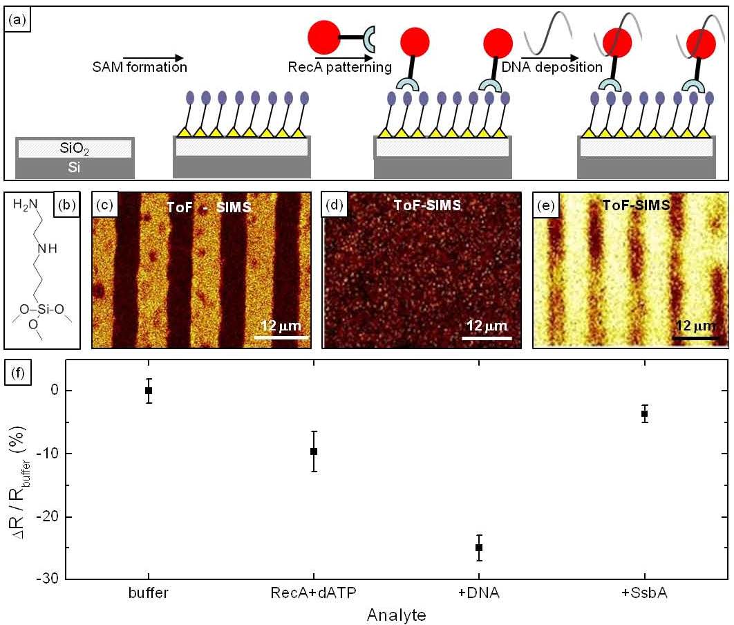
Fig.3. Scheme and images of a Si NW basedBiosensor and scheme of the surface functionalisation of the device and response of the sensor to differentanalites.
4.MoS2 field-effect nanoscale transistors
o-SPL has been applied to pattern dielectric barriers on a MoS2 thin film field-effect transistor to reduce the transistor channel from 2 microns to 200 nm. In this case, o-SPL constitutes a direct and local method to modify the chemical composition of the MoS2 flake.
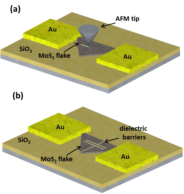
Figure 4. (a) Scheme of the fabrication process of dielectric barriers on a MoS2 flake by o-SPL and (b) of the final device. Figure 5. (a) Optical image of several MoS2 flakes deposited on a 270 nm thick SiO2 layer. (b) AFM phase image of a MoS2 thin layer FET.
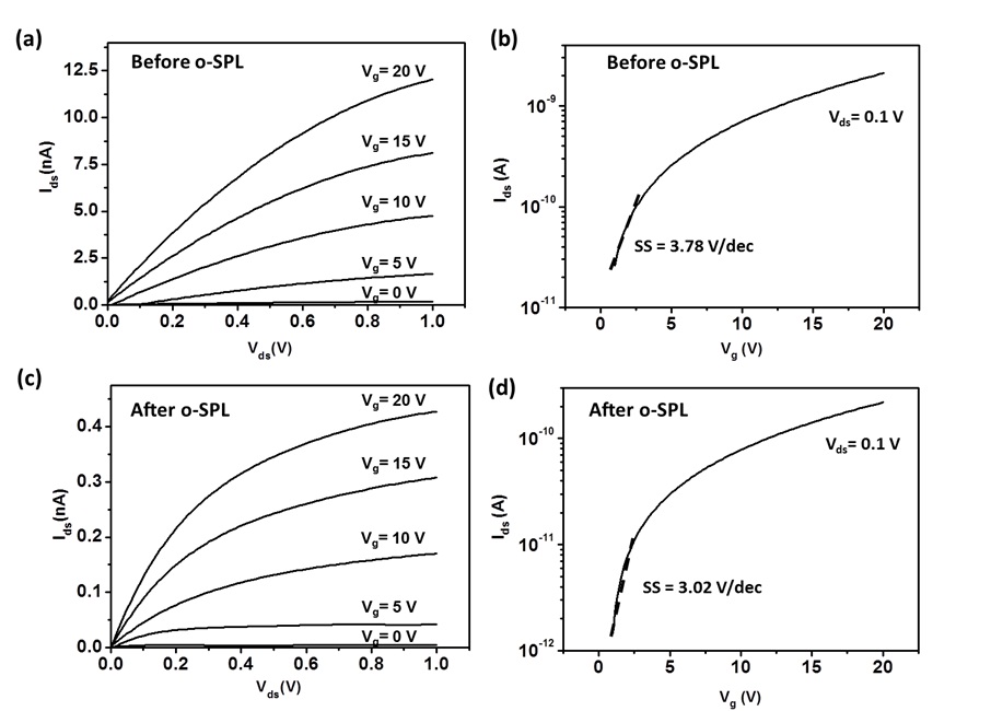
Figure 6. Output and transfer characteristics of a MoS2 FET. (a) Output and (b) transfer curves before the fabrication of dielectric barriers by o-SPL. (c) Output and (d) transfer curves of the nano-FET after o-SPL.
Relevant publications:
- J. Martinez, R. V. Martinez and R. Garcia, Nano Lett., 8, 3636 (2008)
- Y. K. Ryu, M. Chiesa and R. Garcia, 24, 315205 (2013).
- M. Chiesa, P. P. Cardenas, F. Otón, J. Martinez, M. Mas-Torrent, F. Garcia, J. C. Alonso, C. Rovira and R. Garcia, Nano Lett., 12, 1275 (2012)
- F. M. Espinosa, Y. K. Ryu, K. Marinov, D. Dumcenco, A. Kis and R. García, Applied Physics Letters , 106, 103503 (2015)