Advanced Dynamic Atomic Force Microscopy
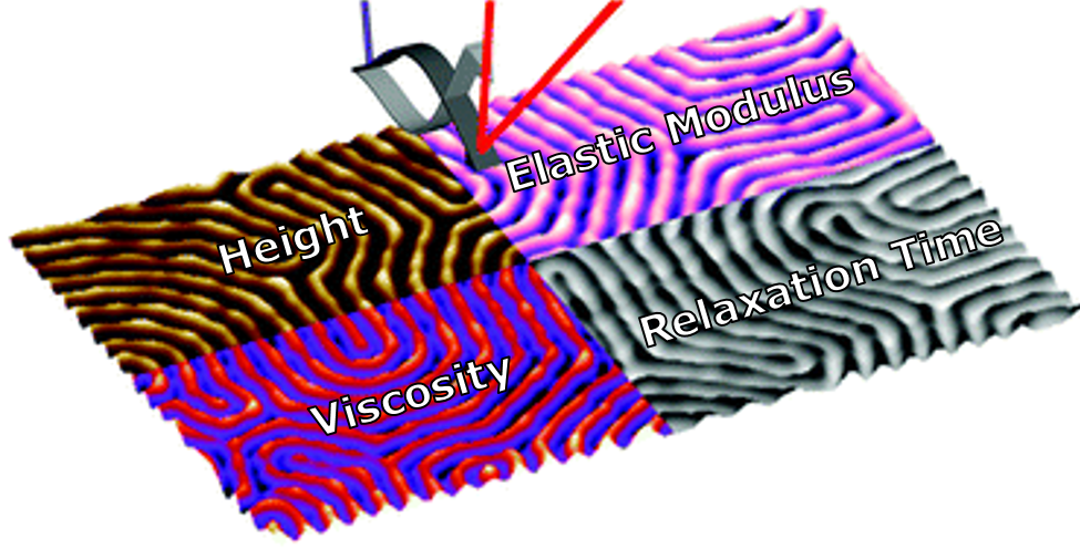
Figure 1. Bimodal AFM nanomechanical maps of PS-b-PMMA block co-polymer. https://doi.org/10.1039/C9NR04396A
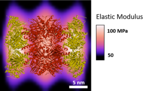
Figure 2. High resolution Bimodal AFM maps of a 20S proteasome in liquid. https://doi.org/10.1038/s41596-018-0070-1
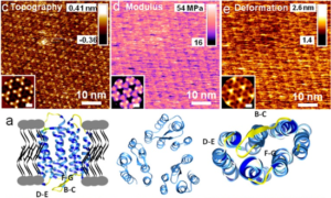
Figure 3. High resolution Bimodal AFM maps of a purple membrane in buffer. https://doi.org/10.1021/acsnano.7b04381
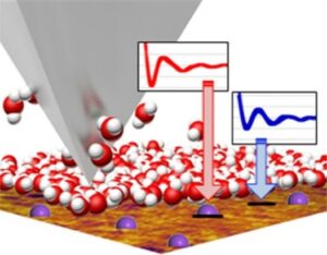
Figure 4. Scheme of the water and cations structure over the mica surface as measured by 3D-AFM. https://doi.org/10.1021/acs.jpclett.7b02671
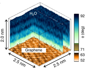
Figure 5. Three-dimensional (3D)-AFM images of 2D Epitaxial graphene grown on SiC. The images show the changes of the phase shift as function of the xyz position. The oscillations are related to changes in the solvent density. Those changes give rise to a layered structure with a few-angstroms features. https://doi.org/10.1038/s41467-019-10740-w
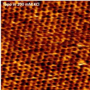
Figure 6. High resolution topographic image of the mica lattice measured in buffer. https://doi.org/10.1038/s41467-019-10740-w
Nanomedicine
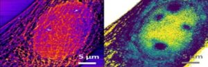
Figure 7. Topography and Young’s Modulus of the actin cytoskeleton in Fibroblast cells, which enables the imaging of cellular organelles inside the nucleus. https://doi.org/10.1021/acsnano.9b04808
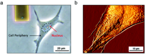
Figure 8. (a) Optical microscopy image of a rectangular microcantilever in the proximity of a fibroblast cell. The black dashed line indicates the edges of the nucleus. The image has been taken using an inverted optical microscope. The pyramidal tip appears at the end of the cantilever. (b) AFM image of a MEF cell. The image reveals the existence of several elements of the cytoskeleton structure. https://doi.org/10.1039/C7NR03419A
Nanofabrication and Nanolithography
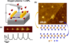
Figure 9. O-SPL patterning and kinetics on pristine WSe2 flakes. (a) AFM topographic image of a line of patterns fabricated at 42% of relative humidity, an applied voltage of 16.2 V and variable pulse times of 0.6, 0.9, 1.2, 1.5, and 1.8 ms (from left to right). Below, the cross section corresponding to the white dashed line is shown. (b) AFM topographic image of o-SPL patterned triangles on two adjacent terraces. The vertical flip shown by the triangles with respect to each terrace reflects the 180° rotation offset between consecutive layers characteristic of TMDC layered materials. https://doi.org/10.1021/acsami.8b15937
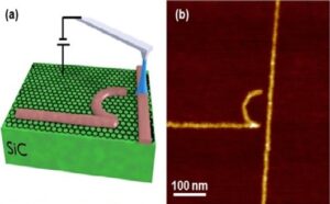
Figure 10. (a) Scheme of o-SPL patterning on a graphene layer formed on SiC. (b) o-SPL pattern on graphene. The narrowest section between the o-SPL patterns is of 18 nm. https://doi.org/10.1016/j.carbon.2017.12.033
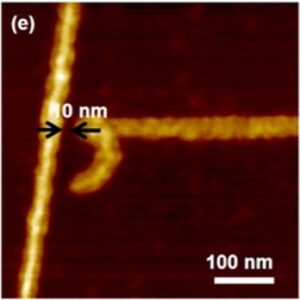
Figure 11. Nano-oxide lines on graphene grown on SiC. The oxide lines define a quantum dot connected with the graphene surface by 10 nm and 22 nm wide constrictions. https://doi.org/10.1088/1361-6528/aa5651