
ENIGMA
ENIGMA Linear and nonlinear photonics with leading-edge materials
PRINCIPAL INVESTIGATORS:
Sánchez Royo, Juan Francisco & Ferrando Cogollos, Albert
ASSOCIATED INVESTIGATOR :
María C. Asensio
TOTAL FUNDING:
590.100,00 €
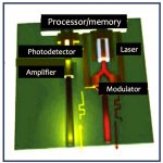
ENIGMA will develop a new generation of photonic elements (or optical devices) able to provide the required functionalities of a Network on a Chip (fast speed transmission, optical routing, and photodetection). Lasers, photodetectors, modulators and routers will be implemented into silicon technology and, for some of the devices, also flexible substrates will be contemplated, as the basis for future “portable”/”wearable” technology. The choice of new materials, multifunctional and with outstanding active and nonlinear properties, will allow us to improve the current figures of merit, or to implement new features not available up to now. The selected materials will be Our project will also explore advanced concepts in photonics (topological insulator photonics) that will be translated to the experimental proposals. Finally, research will also include the optical design of the devices, the optimization of the fabrication techniques and, in some cases, the study of the basic optical/electrical properties of new materials if not known and needed for a given device. The whole proposal is included in the social challenges of the Comunitat Valenciana I+D+I plan, the National Research Plan, and Horizon 2020. Specifically, this research can help in the development of new knowledge and technology (photonics), within the challenge of safe, clean, and efficient energy. The project is also related to the use of low temperature and low-cost processes and materials, which is in line with the challenge of action for the climate, environment, resource efficiency, and raw materials. Besides, since the devices to be developed are applicable both in telecommunications (for future Internet of Things, IoT) and optical sensors, the project could also be included in the challenge of devices for high-speed and low-consumption telecommunications and within the challenge of Security-Defense. Due to the scientific-technical nature of the project, the facilitating technologies involved are Photonics and Nanotechnology, both recognized in the H2020 Challenges.
The main objectives of the project cover the components involved in a Network on a Chip
(1) Light emitting sources with enhanced emission rates,
(2) Photodetection, modulation and routing. All these devices will be based on novel materials of strong interest nowadays for the scientific community (perovskite nanocrystals, 2D/3D perovskites and lead-free perovskites/perovskite-like) with outstanding nonlinear and active properties.