
NEW INSIGHT ON THE ROLE OF LOCALISATION IN THE ELECTRONIC STRUCTURE OF THE SI(111)(7 × 7) SURFACES
SCIENTIFIC CASE
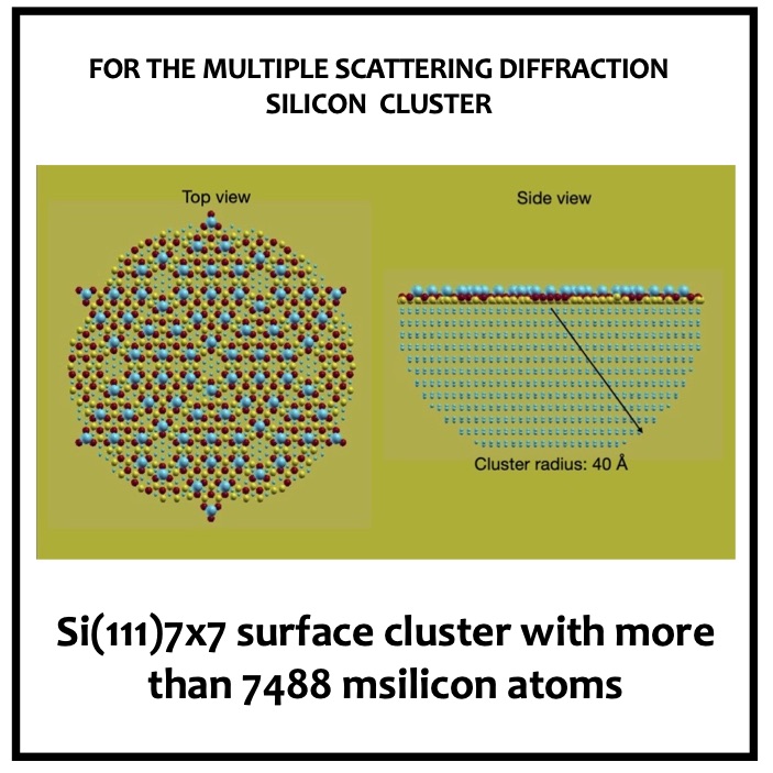


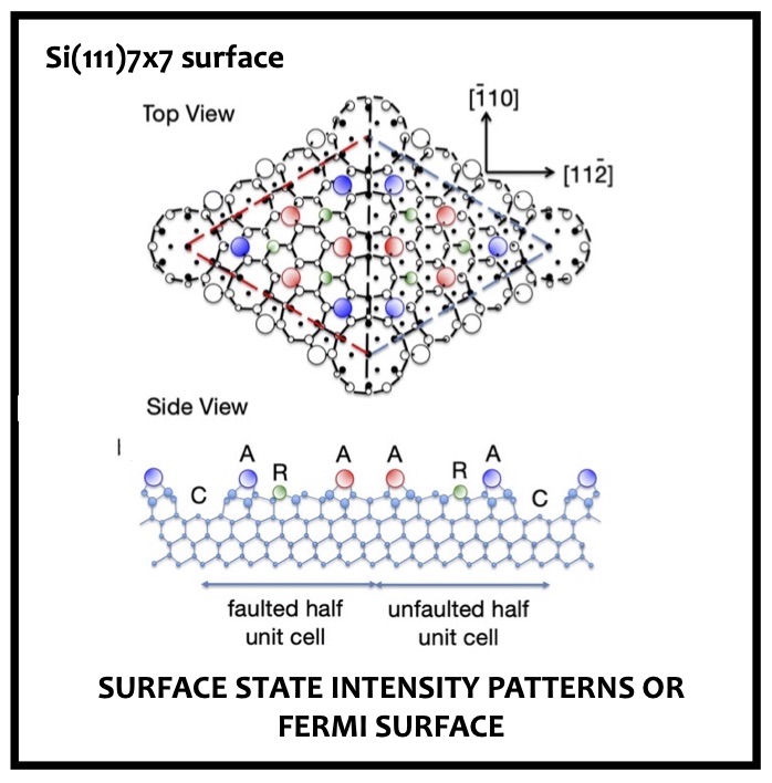
Despite extensive investigation of the 2D electronic structure and conductive properties of the surface of Si(111), in its stable (7 × 7) reconstruction, key aspects remain controversial. The surface reconstruction is well- known to lead to the emergence of two surface localised states, generally labelled S1 and S2, in the bulk band gap of Si, at binding energies relative to the Fermi level of ~ 0.2 eV and ~ 0.8 eV, respectively, although there is evidence that the S1 state is split into 2 or 3 distinct components. These states are generally believed to form 2D itinerant band states and have been extensively studied by ARPES. The widely-accepted structural model of the Si(111)(7 × 7) surface reconstruction is the so-called dimer-adatom-stacking fault (DAS) structural model first proposed by Tagayanaki et al. although very recently alternative polymorphs have been proposed. Within this large unit mesh the number of Si dangling bonds produced by cleavage of the bulk crystal is reduced from 49 to 19 by the associated reconstruction of the outermost Si layers, significantly lowering the surface energy. These remaining dangling bonds are on Si adatoms, bonded to three underlying ‘bulk’ Si atoms, and on ‘rest’ atoms in the lower layer that retain their original dangling bond character. Figure 1 shows the DAS structural model, identifying the local geometry of the adatoms and rest atoms. Charge rearrangement is believed to occur with the six rest atoms and the corner hole rest atom, each accepting one electron from an adatom, leaving the 12 adatoms in the outermost layer with only 5 electrons. This odd number of electrons implies that the surface should be metallic.
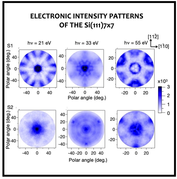
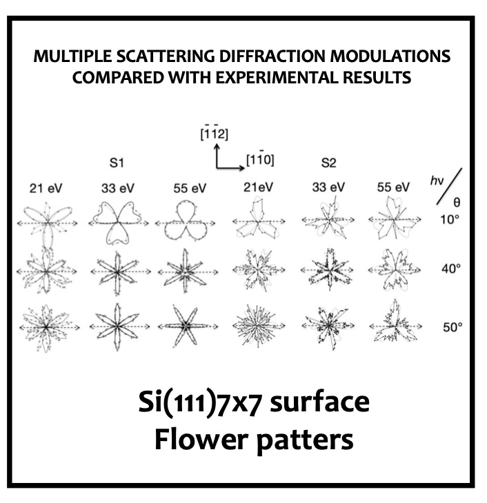
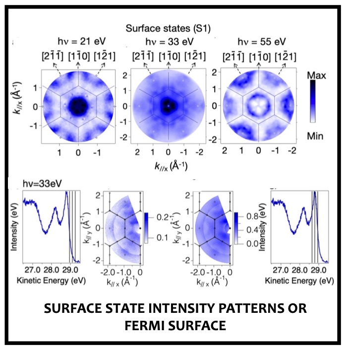
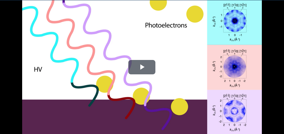
New angle-resolved photoelectron spectroscopy (ARPES) data, recorded at several different photon energies from the Si(111)(7 × 7) surface, show that the well-known S1 and S2 surface states that lie in the bulk band gap are localised at specific (adatom and rest atom) sites on the reconstructed surface. The variations in the photoemission intensity from these states as a function of polar and azimuthal emission angle, and incident photon energy, are not consistent with Fermi surface mapping but are well-described by calculations of the multiple elastic scattering in the final state. This localisation of the most shallowly bound S1 state is consistent with the lack of significant dispersion, with no evidence of Fermi surface crossing, implying that the surface is not, as has been previously proposed, metallic in character. Our findings highlight the importance of final state scattering in interpreting ARPES data, an aspect that is routinely ignored and can lead to misleading conclusions.

AUTHORS: M.E. Dávila, J. Ávila, I.R. Colambo, D.B. Putungan, D.P. Woodruff, M.C. Asensio.
COLLABORATION BETWEEN THE FOLLOWING INSTITUTIONS
- Materials Science Institute of Madrid (ICMM), Spanish Scientific Research Council (CSIC), 28049 Cantoblanco, Madrid, Spain.
- Synchrotron SOLEIL, L’Orme des Merisiers, Saint Aubin-BP 48, 91192 Gif sur Yvette Cedex,
- Institute of Mathematical Sciences and Physics, University of the Philippines Los Baños, 4031 Los Baños, Laguna, Philippines.
- Physics Department, University of Warwick, Coventry CV4 – 7AL, UK.
- MATINEE: CSIC Research Associated Unit Between the Institute of Materials Science of the Valencia University (ICMUV) and the ICMM, 28049 Cantoblanco, Madrid, Spain.*email: mc.asensio@csic.es
CITATION: New insight on the role of localisation in the electronic structure of the Si(111)(7 × 7) surfaces, Sci Rep. 11 (2021) 15034. https://doi.org/10.1038/s41598-021-94664-w.