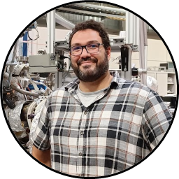
I’m a highly motivated experimental physicist whose career has always been a back and forth between the fascinating worlds of surface physics and nanotechnology. With a strong background in X-ray spectroscopies, growth and characterization of 2D and nanostructured materials and surface physics and chemistry in ultra-high vacuum conditions, I’ve explored the electronic, chemical, and structural properties of complex materials.
I obtained my master’s degree in Physics at Instituto Balseiro (Bariloche, Argentina), in the study of the adsorption and desorption of S and Se form the (111) surface of Ag and Au by dosage in ultra-high vacuum conditions. Then I moved to the National University of Tucumán in the North of Argentina where I made my Ph.D. studying surface properties of semiconductor nanostructures, in particular ZnO nanowires.
After finishing my Ph.D. I became a Postdoctoral Researched at the SuperESCA beamline of the Elettra Synchrotron in Trieste, Italy, for three years. During my tenure there I worked in the study of the growth, structural and electronic properties of two-dimensional materials by means of photoemission with synchrotron radiation and adsorption spectroscopies. I not only conducted cutting-edge research but also collaborated closely with fellow researchers and users of the beamline. This collaborative environment provided invaluable opportunities to engage with international research groups, broadening my expertise across various facets of surface physics and materials science.
Since 2022 I am a Postdoctoral Researcher in the ESISNA Group at the Institute of Materials Science in Madrid (ICMM-CSIC), where my research focuses on the on-surface synthesis of novel two-dimensional materials through light-induced chemical reactions. In addition to all the classic surface science experimental techniques (LEED, XPS, AES, Synchrotron), I’m now specializing in a very powerful tool: the scanning tunneling microscope (STM), both at room temperature and at liquid nitrogen and helium temperatures. With this technique, it is possible to observe molecular self-assemblies on surfaces with atomic resolution, study molecular orbitals and electronic properties, and manipulate matter at the atomic scale.
My journey in experimental physics has been defined by a commitment to pushing boundaries and overcoming challenges. Each and every experiment presents unique technical and experimental requirements that drive innovation and discovery. I’m passionate about advancing the understanding of materials at the atomic and molecular levels and welcome collaborations and inquiries from fellow researchers and enthusiasts in the field.
I invite you to read a bit more about my adventure as a scientist in the following article (Revista CET 44 (2023), in Spanish).

