On 28th and 29th we hold the kickoff meeting of the iLINK0052 project on “Nanorobots and Magnetic sensors based on Nanowires”. This enriching and discussion full meeting was attended by Dr. Olga Kazakova (NPL, Teddington, UK), Ass. Prof. Jürgen Kosel (KAUST, Saudi Arabia), Ass. Prof. Dieter Suess (University of Vienna), Dr. Xiangzhong Chen (ETH, Zurich), Dr. Christoph Vogler (University of Vienna) apart from staff members of ICMM/CSIC Manuel Vazquez, Agustina Asenjo, Oksana Chubykalo-Fesenko, Cristina Bran, Rafael Perez, David Navas, Alfredo Jacas, and Prof. Laura H. Lewis from Northeastern University, Boston.
New excursion of the group
The traditional summer excursion of the group took place June 26th to visit Sigüenza, the old Castilian city which origin goes back to the Celtiberian Segontia. After the 2 hours walk by the pines and under a suffocating sun to the nearby Natural Park, we had a comforting lunch. It was followed by the cultural visit to the medieval Castle and the gothic Cathedral that hosts the famous tomb of the Doncel.

New paper of the group
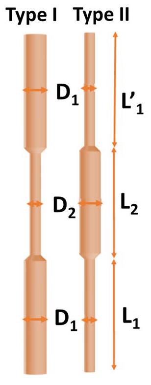
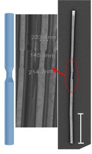
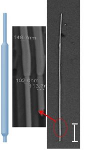
“Geometrically designed domain wall trap in tri-segmented nickel magnetic nanowires for spintronics devices”
Farzad Nasirpouri, Seyed-Majid Peighambari-Sattari, Cristina Bran, Ester M. Palmero, Eider Berganza Eguiarte, Manuel Vazquez, Aristotelis Patsopoulos and Dimitris Kechrakos, Scientific Reports (2019) 9:9010 | https://doi.org/10.1038/s41598-019-45553-w
“Domain wall traps” have been engineered diameter-modulated (DM) cylindrical magnetic nanowires (NWs). A systematic study on the magnetization behavior, domain wall structure and its nucleation/propagation in tri-segmented diameter-modulated Ni nanowires was performed to investigate the magnetization reversal as function of segment geometry. Two distinct geometries include: dumbbell-type (type I) and rolling pin-type (type II). Based on experimental and theoretical simulations, it was evidenced that the wide-narrow junctions create trap sites for domain walls where the narrow segment restricts their motion. This type of geometrically engineered nanowires exhibit potential efficiency for future novel spintronic devices in particular when assembled in arrays as a practical 2D memory devices.

New european patent
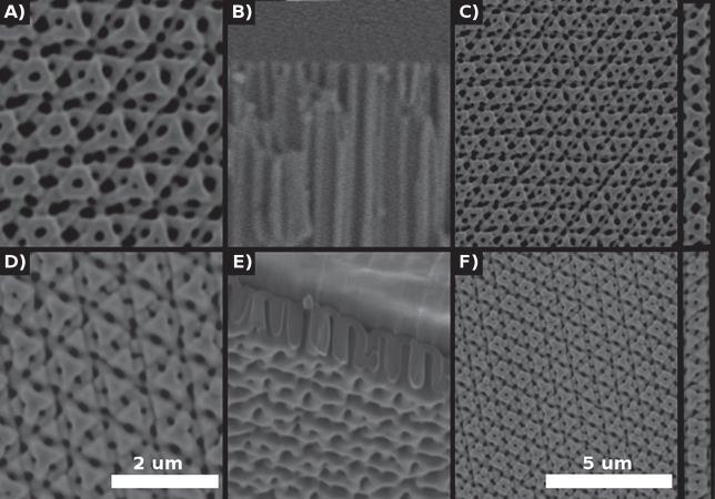
The European Union patent EP19382510 has been filed with the title “Method for nanostructured materials fabrication combining soft lithographic imprint, aluminium anodization and metal sputtering” by Manuel Vazquez (ICMM/CSIC), David Gonzalez (ICMM/CSIC) and David Navas (Porto University).