“Continuous and nanopatterned TbCo based heterostructures with in-plane and perpendicular anisotropy”
Nikita A. Kulesh, PhD by the Autonomous University of Madrid (Sobresaliente cum laude), supervised by Manuel Vázquez and Vladimir O. Vaskovskii
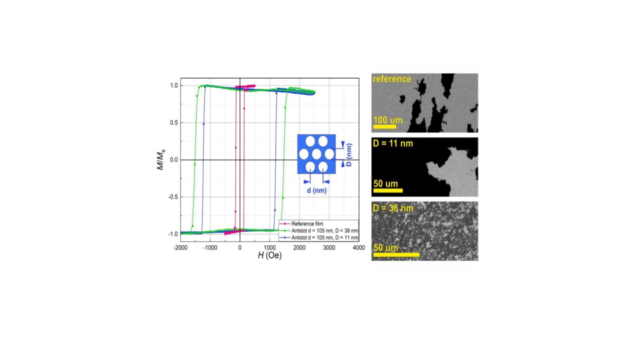
This thesis focuses on investigation of magnetic properties and magnetization reversal processes in continuous and antidot patterned TbCo ferrimagnetic amorphous films with perpendicular magnetic anisotropy (PMA). The search for new ways of tailoring magnetic anisotropy and hysteresis properties of magnetic films with PMA by adjusting their shape at the nanoscale level is the main objective.
In the first part, magnetic properties of amorphous TbCo films are investigated using auxiliary systems with simpler magnetic structures LaCo and GdCo. A possibility to produce TbCo layers having the same composition but different character of magnetic anisotropy is demonstrated. TbCo layers with PMA or in-plane magnetic anisotropy were used to induce unidirectional anisotropy in adjoining FeNi layers.
In the last part, micromagnetic simulation is employed to analyze and reproduce experimental results obtained for TbCo and GdCo antidot patterned films. An approach of step-by-step complication of micromagnetic model is used so separate and analyze sources of experimentally observed variations in magnetization processes.

This PhD research study derives from the collaboration with the Department of Magnetism and Magnetic Nanomaterials, Urals Federal University in Ekaterinburg.