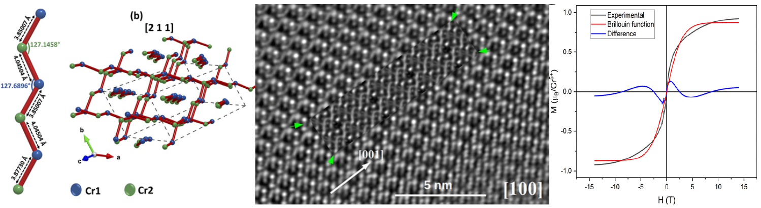
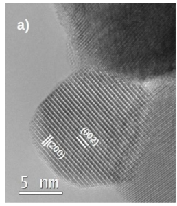
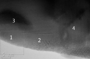
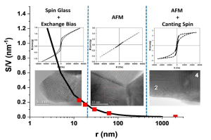
Growth of out-of-plane standing MoTe2(1−x)Se2x/MoSe2 composite flake films by sol-gel nucleation of MoOy and isothermal closed space telluro-selenization

A. Fernández García, V. Torres-Costa, O. de Melo, F. Agulló-Rueda, G. R. Castro and M. Manso Silvan, “Growth of out-of-plane standing MoTe2(1−x)Se2x/MoSe2 composite flake films by sol-gel nucleation of MoOy and isothermal closed space telluro-selenization,” Appl. Surf. Sci. 546, 149076 (2021)

Publicado en nanocharacterization, nanoscience, nanotechnology, Publications, Raman spectroscopy, semiconductor | Etiquetado , , , | Comentarios desactivados en Growth of out-of-plane standing MoTe2(1−x)Se2x/MoSe2 composite flake films by sol-gel nucleation of MoOy and isothermal closed space telluro-selenization

Fabrication and characterization of nanostructured porous silicon-silver composite layers by cyclic deposition: dip-coating vs spin-coating

N. Naveas, M. Manso-Silván, R. Pulido, F. Agulló-Rueda, V. Torres-Costa, T. Plaza, H. Pesenti, G. Recio, and J. Hernandez-Montelongo, “Fabrication and characterization of nanostructured porous silicon-silver composite layers by cyclic deposition: dip-coating vs spin-coating,“ Nanotechnol. 31, 365704 (2020)

Publicado en microscopy, nanocharacterization, nanoscience, nanotechnology, Publications, Raman spectroscopy, silicon | Etiquetado , , , | Comentarios desactivados en Fabrication and characterization of nanostructured porous silicon-silver composite layers by cyclic deposition: dip-coating vs spin-coating

Laser writing of nanostructured silicon arrays for the SERS detection of biomolecules with inhibited oxidation

P. Pellacani, V. Torres-Costa, F. Agulló-Rueda, R. Vanna, C. Morasso, M. Manso Silván, “Laser writing of nanostructured silicon arrays for the SERS detection of biomolecules with inhibited oxidation,” Colloids Surf. B 174, 174–180 (2019)

Publicado en laser irradiation, microscopy, nanocharacterization, nanoscience, nanotechnology, Publications, Raman spectroscopy, silicon | Etiquetado , , , , , , , , | Comentarios desactivados en Laser writing of nanostructured silicon arrays for the SERS detection of biomolecules with inhibited oxidation

Nanostructural changes upon substitutional Al doping in ZnO sputtered films

A. R. Landa-Cánovas, J. Santiso, F. Agulló-Rueda, P. Herrero, E. Navarrete-Astorga, E. Ochoa-Martínez, J. R. Ramos-Barrado, and M. Gabás, “Nanostructural changes upon substitutional Al doping in ZnO sputtered films,” Ceram. Int. 45, 6319–6327 (2019).

Al:ZnO layers, with low and high Al content, 0.2% and 2.1% cat. respectively, have been prepared using the RF magnetron sputtering technique. Noticeable differences in the optical and electrical properties have been detected in these films. With doping, the resistivity decreases and the band-gap increases. The alterations in the films crystalline structure are explained in terms of the nanostructural changes induced by Al substitutional doping, such as a higher concentration of edge dislocation defects and a higher rotation of crystalline nanodomains in the plane of the films (normal to the preferential orientation c-axis) for the high content Al:ZnO layer. A complete description of such effects has been accomplished using several characterization techniques, such as X-ray diffraction, Raman spectroscopy and transmission electron microscopy. The combination of these techniques provides an exhaustive understanding of the films nanostructure.

Publicado en HRTEM, microscopy, nanocharacterization, nanoscience, Publications, Raman spectroscopy, transparent conductive oxides, zinc oxide | Etiquetado , , , , , , , , | Comentarios desactivados en Nanostructural changes upon substitutional Al doping in ZnO sputtered films

Laser writing of nanostructured silicon arrays for the SERS detection of biomolecules with inhibited oxidation

P. Pellacani, V. Torres-Costa, F. Agulló-Rueda, R. Vanna, C. Morasso, M. Manso Silván, “Laser writing of nanostructured silicon arrays for the SERS detection of biomolecules with inhibited oxidation,” Colloids Surf., B, accepted (2018).

The present work reports the processing of laser irradiated Si arrays (LISi) and underlines their surface enhanced Raman scattering (SERS) functionality. A nanostructured Si/SiOx surface forms providing additional fluidic and photoprotective properties. Because of their optical and surface characteristics, the arrays exhibit a SERS analytical enhancing factor of 500, without any noble metals such as gold or silver. Micro-Raman maps allowed studying LISi properties, identifying maximum amplification in nanostructured areas characterized by the presence of 7 nm Si nanocrystals. These structures are confined by a SiOx layer as illustrated by XPS valence band measurements. The highly hydrophilic LISi areas allow a pre-concentration of target molecules prior to SERS analysis. A relevant application of LISi was found in the detection of apomorphine (APO), a drug used for the treatment of Parkinson’s disease. In contrast with what is obtained by using gold SERS substrates, LISi allows the detection of APO with no sign of oxidation. This invites for the use of the Si/SiOx SERS detection in future systems for the personalized delivery of APO.

Publicado en microscopy, nanocharacterization, nanoscience, nanotechnology, Publications, Raman spectroscopy, silicon | Etiquetado , , , , , , | Comentarios desactivados en Laser writing of nanostructured silicon arrays for the SERS detection of biomolecules with inhibited oxidation

Lattice damage in 9-MeV-carbon irradiated diamond and its recovery after annealing

DiamondCarbon20170421.resizedF. Agulló-Rueda, N. Gordillo, M. D. Ynsa, A. Maira, J. Cañas, and M. A. Ramos, “Lattice damage in 9-MeV-carbon irradiated diamond and its recovery after annealing,” Carbon , accepted (2017).

We have studied the radiation damage in diamond as a function of layer depth upon self-ion implantation with 9-MeV carbon ions and its recovery after annealing at 1000°C. Raman and photoluminescence spectra show substantial damage of the lattice, namely, amorphization, neutral vacancies, and interstitial defects. Damage is maximum in the stopping layer at a depth of 4 μm. After annealing there is some recovery of the lattice, but the residual damage increases with fluence, up to about 2 × 1016 ions/cm2. At this fluence the stopping layer becomes highly disordered and does not heal with annealing. Surprisingly, for higher fluence values, of about 5 × 1016 ions/cm2, there is almost no residual damage. After full amorphization is reached, the layers appear to recrystallize by solid phase epitaxy (SPE), using the pristine diamond layers underneath as a template. These results prove that graphitization of diamond after annealing can be avoided in deeply buried layers, implanted at fluences much higher than expected. High fluences, in fact, can lead to high quality diamond layers. If SPE can be confirmed, it would have a great interest for diamond device applications, as it allows for higher doping levels.

Publicado en diamond, ion irradiation, microscopy, nanocharacterization, photoluminescence, Publications, Raman spectroscopy | Etiquetado , , , , , , | Comentarios desactivados en Lattice damage in 9-MeV-carbon irradiated diamond and its recovery after annealing

Characterization of the interface between highly conductive Ga:ZnO films and the silicon substrate

Work in collaboration with the Nanotech Unit, Department of Applied Physics I, University of Malaga, Spain.

M. Gabás, E. Ochoa-Martínez, E. Navarrete-Astorga, A. R. Landa-Cánovas, P. Herrero, F. Agulló-Rueda, S. Palanco, J. J. Martínez-Serrano, and J. R. Ramos-Barrado, “Characterization of the interface between highly conductive Ga:ZnO films and the silicon substrate,” Appl. Surf. Sci. 419, 595–602 (2017)

Gallium-doped zinc oxide films are an interesting alternative for transparent conductive materials. To improve their performance, the interface between the grown layer and the substrate must be fully understood. Accordingly, ZnO and Ga:ZnO films have been deposited onto p-type doped Si (111) substrates by magnetron sputtering for 1, 2, 3 and 20 min and their interfaces characterized by transmission electron microscopy, photoelectron spectroscopy, spectroscopic ellipsometry and impedance spectroscopy. The combination of transmission electron microscopy techniques suggested a more complex interface chemistry in the Ga:ZnO/Si case, a point confirmed by x-ray photoelectron spectroscopy measurements on very thin films. While the ZnO/Si interface consists mostly of silicon oxides, zinc silicates and some Zn0, the Ga:ZnO/Si interface, besides these constituents, has a noticeable amount of Ga:ZnO and small quantities of Ga0. The band alignment deduced from the photoelectron spectroscopy measurements, together with the layers and Si band gap values, evidences a higher work function for the doped film and a smaller conduction band barrier for the Ga:ZnO/Si interface. Concerning the optical and electrical characteristics, spectroscopic ellipsometry revealed no significant differences between the two interfaces, while impedance spectroscopy measurements demonstrated that the Ga:ZnO/Si interface is less resistive than the ZnO/Si one.

Publicado en HRTEM, microscopy, nanocharacterization, nanoscience, nanotechnology, Publications, transparent conductive oxides, zinc oxide | Etiquetado , , , , , , , | Comentarios desactivados en Characterization of the interface between highly conductive Ga:ZnO films and the silicon substrate

Micro-Raman spectroscopy of near-surface damage in diamond irradiated with 9-MeV boron ions

F. Agulló-Rueda, M. D. Ynsa, N. Gordillo, A. Maira, D. Moreno-Cerrada, and M. A. Ramos, “Micro-Raman spectroscopy of near-surface damage in diamond irradiated with 9-MeV boron ions,” Diamond Relat. Mater. 72, 94–98 (2017)

GraphicalAbstract2016DRM04smallWe have studied the near-surface damage in a diamond crystal caused by irradiation with swift boron ions and its healing after high-temperature annealing. A diamond crystal was irradiated with 9-MeV 11B3 + ions with fluence values between 1 × 1015 and 4.42 × 1016 ions/cm2 to generate various levels of lattice damage. The ions loose energy to the lattice and, according to simulations, stop at a depth of about 5 μm, where they form a thin buried implantation layer. For the near-surface layers damage is produced by the ions at high kinetic energy before they slow down. Only intrinsic defects can be produced, with no boron atoms. The lattice damage of the near-surface layers and its recovery after annealing for 1 hour at 1000°C were studied by Raman and photoluminescence spectroscopies. Back-scattered light from a 514.5-nm laser beam was collected from the sample surface, probing a depth of a few micrometers. We observe some disordering of the lattice plus the formation of neutral vacancies, interstitial and other lattice defects. After annealing the Raman spectrum shows a significant recovery of the lattice order and the disappearance of isolated neutral vacancies. Residual damage is confirmed by the luminescence spectrum, that shows the appearance of new spectral features.

Publicado en diamond, ion irradiation, microscopy, nanocharacterization, photoluminescence, Raman spectroscopy | Etiquetado , , , , | Comentarios desactivados en Micro-Raman spectroscopy of near-surface damage in diamond irradiated with 9-MeV boron ions

Study of the formation mechanism of hierarchical silicon structures produced by sequential ion beam irradiation and anodic etching

In a collaboration with the Autonomous University of Madrid (Department of Applied Physics and the Center for Micro Analysis of Materials) and the Institut für Solarenergieforschung Hameln (ISFH) of Germany we have studied the formation of micropatterns combining nanostructured (porous) Si (NPSi) and bulk Si by a sequential process of selective high energy ion irradiation and anodic etching.

E. Punzón Quijorna, S. Kajari-Shrönder, F. Agulló-Rueda, M. Manso Silván, R. J. Martín Palma, P. Herrero Fernández, V. Torres-Costa, and A. Climent, “Study of the formation mechanism of hierarchical silicon structures produced by sequential ion beam irradiation and anodic etching,” Vacuum 138, 238–243 (2017).

Publicado en HRTEM, ion irradiation, microscopy, nanocharacterization, nanoscience, nanotechnology, Raman spectroscopy, silicon | Etiquetado , , , , , , | Comentarios desactivados en Study of the formation mechanism of hierarchical silicon structures produced by sequential ion beam irradiation and anodic etching

Direct laser writing of nanorough cell microbarriers

In collaboration with the Advanced Photonic and Biofunctional Materials group the Autonomous University of Madrid, lead by Dr. Miguel Manso, we have studied by Raman microspectroscopy laser written silicon-based structures for biological cell microbarriers.

Y. Xiang, R. Martínez Martínez, V. Torres-Costa, F. Agulló-Rueda, J. P. Garcia-Ruiz, and M. Manso Silván, «Direct laser writing of nanorough cell microbarriers on anatase/Si and graphite/Si,» Mater. Sci. Eng. C 66, 8–15 (2016)

Publicado en microscopy, nanocharacterization, nanoscience, nanotechnology, Publications, Raman spectroscopy, silicon | Etiquetado , , , , , | Deja un comentario