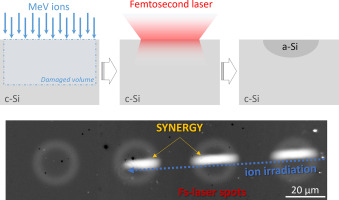
Osteosarcoma is a radioresistant cancer and proton therapy a promising radiation alternative to treat cancer with the advantage of high dose concentration in the tumor area. In this work, we propose the use of iodine substituted hydroxyapatite nanomaterials (IHAP) to use iodine (127I) as a proton radiation tracer giving access to range verification studies in mineralized tissues. For this purpose, the nanomaterials were synthesized at four iodine concentrations by hydrothermal synthesis. The material is characterized using different microstructural techniques to identify an optimal high iodine concentration and pure apatite phase nanomaterial. Finally, such pure IHAP powders were shaped and irradiated with proton beams of 6 and 10 MeV and their activation demonstrated through subsequent decay analysis. The materials could be integrated in phantom structures for the verification of doses and range of protons prior to animal testing and clinical proton therapy treatments of tumors located deep under combined soft and calcified tissue.
R. Magro, A. Muñoz-Noval, J. A. Briz Monago, J. R. Murias, A. Espinosa Rodríguez, L. M. Fraile, F. Agulló-Rueda, M. D. Ynsa, C. Tavares de Sousa, B. Cortés Llanos, G. M. García López, E. Nacher, V. García Tavora, N. Mont i Geli, A. Nerio, V. Valladolid Onecha, R. Pallás, A. Tarifeno-Saldivia, O. Tengblad, M. J. Manso Silvan and S. Viñals i Onsés, «Iodine substituted hydroxyapatite nanoparticles and activation of derived ceramics for range verification in proton therapy,» J. Mater. Chem. B , (2024).